In server builds with GPUs and NVMe, “PCIe lanes” are not an abstract line in a spec sheet — they’re a real resource that determines how many devices you can connect without losing speed, how predictably the system will scale, and how easily you’ll be able to expand it later. A PCIe planning mistake rarely shows up as “minus 10%” — more often it triggers a chain reaction: GPUs suddenly run at x8 instead of x16, some NVMe drives end up “behind the chipset” and hit an uplink ceiling, and when you add one more card the whole system starts degrading for seemingly no reason.
A typical story: you buy a server for 4× GPUs + NVMe for a dataset; on paper, by “slot count,” everything looks perfect. But in practice one riser hangs off a switch with oversubscription, two slots share one x16, half of the U.2/EDSFF bays go through the PCH, and BIOS options are enabled that disable peer‑to‑peer or force the link to downshift. You end up with an expensive system that behaves like a cheaper one — and this is almost always fixed at the platform and topology selection stage, not after delivery. Sounds confusing? Let’s break it down.
PCIe, engineering-accurate: Gen, width, lanes, real throughput
A PCIe lane is a pair of high‑speed differential channels “there” and “back.” Important: PCIe is a full‑duplex interface — under normal operation, traffic can flow simultaneously in both directions.
Link width is the number of lanes bundled into a single link: x1 / x4 / x8 / x16. If a device and slot are physically x16, that still does not guarantee the link will actually train at x16.
Generation (PCIe Gen) sets the per‑lane signaling rate. Each new generation roughly doubles throughput, but real systems have caveats:
- a link may train at below the maximum Gen (downtraining) if signal integrity is poor (riser/retimer/trace length/contacts);
- a link may train at less than full width (for example, x8 instead of x16) if lanes are limited or the board is wired that way.
The key takeaway: a physical “x16 slot” ≠ an electrical “x16 link”.
PCIe Gen and throughput (order of magnitude)
| PCIe Gen | Rate per lane (theoretical) | Usable throughput (approx., per direction) | Approx. x4 (per direction) | Approx. x16 (per direction) | Typical devices |
| Gen3 | 8 GT/s | about 1 GB/s per lane | ~4 GB/s | ~16 GB/s | NVMe (older), 25/40/100G NICs, some GPUs/accelerators |
| Gen4 | 16 GT/s | about 2 GB/s per lane | ~8 GB/s | ~32 GB/s | Gen4 NVMe, PCIe GPUs, 100/200G NICs |
| Gen5 | 32 GT/s | about 4 GB/s per lane | ~16 GB/s | ~64 GB/s | Gen5 NVMe, modern GPUs/FPGAs, 200/400G NICs |
| Gen6 | 64 GT/s | about 8 GB/s per lane | ~32 GB/s | ~128 GB/s | AI/HPC platforms/fabrics, disaggregation, future NVMe/CXL |
Practical interpretation: x8 Gen5 (~32 GB/s one way) is often comparable to x16 Gen4 (~32 GB/s) — but only if topology, switch/uplink, NUMA locality, and BIOS settings don’t break the picture.
Where lanes come from: CPU lanes vs chipset (PCH) lanes — and why this breaks expectations

In a server, PCIe lanes “come” from two places:
- CPU PCIe lanes — the most valuable ones:
- lowest latency and the most predictable bandwidth;
- these are what you usually want for GPUs, 200/400G NICs, and NVMe directly attached to the CPU.
- Chipset / PCH lanes — often “cheaper,” because they almost always traverse a shared CPU↔PCH uplink (analogous to DMI/other platform interconnects). That means:
- devices share a common path to the CPU;
- with multiple NVMe drives/controllers under load, you may hit an uplink bottleneck rather than “x4 per drive.”
Common traps:
- a “second M.2” or an extra controller steals lanes from another slot/port;
- you have many slots, but half of them are behind the PCH or share one lane group;
- a U.2/EDSFF cage looks like “tons of NVMe,” but in fact it’s aggregated via a switch/hub with a limited uplink.
Platform “lane budget” — why it changes the entire design
Different platforms have radically different lane budgets, and that directly affects how “honestly” you can connect GPUs + NVMe:
- Intel 5th Gen Xeon Scalable: advertised up to 80 PCIe 5.0 lanes
- AMD EPYC 9004 (Genoa/Bergamo): AMD materials and the white paper cite 128 PCIe Gen5 lanes (in 1P configurations)
This isn’t “marketing math”: the difference between 80 and 128 lanes is the difference between “4× GPUs + some NVMe” and “4× GPUs + lots of NVMe + a fast NIC with no compromises.” Otherwise you have to rely on switches and live with oversubscription (when devices are ready to consume lanes, but the lanes don’t physically exist).
Why PCIe matters for GPUs: not just bandwidth, but topology
When PCIe bandwidth really matters for GPUs
PCIe bandwidth impacts GPU performance the most in scenarios where data constantly moves between CPU/memory and the GPU:
- AI training/inference with frequent H2D/D2H (host‑to‑device / device‑to‑host) transfers;
- streaming pipelines: decode/preprocess on CPU → batches to GPU;
- multi‑GPU setups where some traffic goes “the long way” due to poor socket locality or P2P constraints.
When bandwidth is less critical
If data stays in VRAM for a long time and host transfers are minimal, the drop from x16 to x8 may barely show up:
- compute‑dense kernels;
- batches fit in VRAM and are reused many times;
- the CPU is mostly an “orchestrator,” not a constant data source.
PCIe vs NVLink: realistic expectations for multi‑GPU scaling
It’s important to distinguish:
- CPU↔GPU (usually PCIe)
- GPU↔GPU (PCIe P2P or NVLink/analog)
For example, on the NVIDIA A100 product page, NVIDIA explicitly contrasts PCIe Gen4: 64 GB/s with NVLink: 600 GB/s (for a pair of GPUs). That helps explain why:
- adding GPUs can scale training/parallel workloads “almost linearly” in NVLink topologies,
- but with poor PCIe/NUMA topology you can hit a bottleneck during data loading, synchronization, or pipelines without sufficient locality.
How to read a GPU spec
In the datasheet/product page, check:
- PCIe Gen (4/5) and supported width (x16 or x8);
- NVLink/other interconnect availability (if GPU↔GPU connectivity matters);
- BAR/address space requirements (important for BIOS settings, covered below).
Why PCIe matters for NVMe: x4 links, queues, parallelism, and “how many drives you can attach without surprises”
NVMe is a protocol (a specification describing how non‑volatile memory and command queues work), while PCIe is the interface (the transport that carries those commands and data). This is formalized in the NVM Express NVMe‑over‑PCIe specifications.
Practical basics:
- one NVMe SSD is almost always connected as PCIe x4;
- so 4 NVMe = 16 lanes, 8 NVMe = 32 lanes, 16 NVMe = 64 lanes — and that’s just “ideal math,” not counting NICs/GPUs/controllers.
Why NVMe can be slower than expected in real life, even if “there are enough lanes”:
- PCH/uplink: drives behind the chipset share a common path to the CPU;
- switch/uplink: many ports “down” (to devices) but a narrow “up” link to the CPU (oversubscription);
- thermals: Gen5 NVMe easily hits cooling limits and throttles;
- queues/parallelism: a single thread/queue rarely saturates an NVMe array, and NUMA distance adds latency.
Topology in dual‑socket servers: NUMA, “remote” PCIe, and the cost of crossing sockets

In a dual‑socket system, devices are typically “attached” to a specific CPU: some slots/risers hang off socket 1, others off socket 2. If a process on CPU1 actively reads from an NVMe device connected to CPU2, the data must traverse the inter‑socket interconnect (UPI/Infinity Fabric), adding:
- extra latency,
- less predictable bandwidth under load,
- results that depend on process/IRQ affinity.
The locality principle:
- keep the data source and consumer as close as possible: NVMe ↔ GPU ↔ CPU within the same socket if that’s your critical path.
Symptoms of NUMA mistakes:
- different benchmark results depending on socket/NUMA node;
- “floating” throughput with no obvious reason;
- a sharp drop after adding a second GPU or a second NVMe cage (when traffic starts going “over the bridge”).
PCIe switch / retimer / riser: when they help — and when they create a bottleneck
Why PCIe switches are used
A PCIe switch increases the number of downstream ports — this is the basis of dense NVMe backplanes and sometimes GPU expansion boxes. But a switch doesn’t cancel physics: it still has an uplink to the CPU/root complex.
Broadcom (PLX) is a common supplier for such solutions; the PEX88000 family is a widely used example of server‑class PCIe switches.
Oversubscription, in plain terms
This is when the total potential bandwidth “down” (to devices) exceeds the bandwidth “up” (to the CPU). For example:
- down: 16 NVMe × x4 Gen4 (a lot of potential bandwidth),
- up: one x16 Gen4 uplink.
While devices aren’t busy at the same time, everything looks fine. As soon as the workload becomes parallel, “mysterious degradation” appears.
“Non‑blocking” — what it means in practice
Often, “non‑blocking” refers to the switch’s internal fabric, but it does not remove uplink limits. What you need to verify is the uplink/downlink ratio and how port groups are aggregated.
Retimers/risers/cables
For Gen5/Gen6, link quality is critical. A riser that “looks the same” can:
- degrade signal integrity,
- cause downtraining (Gen5 → Gen4),
- create link instability under load.
OCP is evolving requirements for external PCIe connectivity and retimers as an industry trend (including for NVMe/CXL disaggregation).
BIOS/firmware settings that most often “kill” lanes and devices
Below is a checklist of settings that genuinely affect how the link trains and how GPUs/NVMe/virtualization behave:
- PCIe Link Speed (Auto/force Gen4/Gen5):Auto isn’t always best — but forcing Gen5 on a marginal path can cause instability and fallback behavior.
- Lane bifurcation (x16 → 2×x8 / 4×x4):critical for risers and “4‑NVMe on one x16” adapters.
- Above 4G Decoding:often required for multi‑GPU builds and large BAR mappings.
- Resizable BAR:relevant for some CPU↔GPU transfer patterns (context‑dependent; varies by platform/software).
- SR‑IOV:for NIC virtualization when you need VF splitting.
- ACS/ARI:affects isolation and routing; can hinder P2P, but is often needed for virtualization/security.
- IOMMU / VT‑d / AMD‑Vi:required for passthrough (GPU/NVMe/NIC into VMs).
- ASPM/power saving:often disabled in servers for stability and predictable latency.
Practical lane sizing: “how many GPUs and NVMe can I really run”

Before the scenarios — one simple rule: first do the ideal lane math, then verify the topology (which socket, what exactly it goes through, and what the uplink is).
Scenario 1: 2× GPU + 4× NVMe + 200GbE NIC (AI inference / analytics)
A typical “healthy” target without compromises:
- 2× GPU: most often 2×x16 (or x8 Gen5 — if intentional)
- 4× NVMe: 4×x4 = 16 lanes
- 200GbE NIC: often x16 or x8 (depends on the card)
Total: roughly 64–80 lanes for I/O, plus headroom for controllers/additional NVMe. On platforms with a smaller lane budget, you’ll quickly start sharing slots or using switches.
Scenario 2: 4× GPU + 8–16× NVMe (dense AI box / local dataset)
Ideal math:
- 4× GPU × x16 = 64 lanes
- 8× NVMe = 32 lanes (or 16× NVMe = 64 lanes)
Even without a NIC, that’s already 96–128 lanes. Here you most often see:
- GPUs at x8 instead of x16 (sometimes fine if Gen5 and planned),
- NVMe behind a switch with oversubscription,
- half the NVMe cage on the other socket → NUMA penalty.
Scenario 3: NVMe‑heavy: 24× NVMe in 2U (storage/cache tier)
24 drives × x4 = 96 lanes — almost never routed “straight” to the CPU(s). Typically you’ll see:
- multiple switches,
- backplane partitioning into domains,
- one or more uplinks to the CPU(s),
- and it becomes crucial to understand where oversubscription begins and how it affects your real workload profile.
Approximate lane budget and priorities
| Device | Typical link | Sensitivity to Gen/width | Preferred attachment |
| GPU | x16 (sometimes x8) | High if there’s lots of H2D/D2H, streaming, tight‑coupled pipelines | CPU lanes, ideally socket‑local; consider P2P/NVLink |
| NVMe SSD | x4 | Medium/high: depends on parallelism and I/O profile; Gen5 is very thermals‑sensitive | CPU lanes for predictability; via a switch only if you understand uplink/oversubscription |
| 100/200/400G NIC | x8/x16 | High for high PPS/low latency and large flows | CPU lanes, socket locality matters |
| HBA/RAID/controllers | x8 | Medium | CPU lanes or PCH (if moderate load), but watch the uplink |
Diagnostics: how to tell PCIe is already limiting you

Symptoms
- The GPU runs at x8/x4 instead of x16.
- NVMe doesn’t reach expected speeds, or the throughput graph “saws.”
- Big performance differences depending on slot/riser.
- Degradation after adding a second card or a second U.2/EDSFF backplane.
- Gen5 falls back to Gen4/Gen3, or the link is unstable.
Symptom → likely cause → first thing to do
| Symptom | Likely cause | What to do first |
| “Physically x16, but effectively x8” | lane shortage, slot sharing, board wiring, BIOS settings | check the board block diagram/manual; verify bifurcation and neighboring slot interactions |
| NVMe slower than expected | behind PCH/uplink, switch uplink, thermal throttling | move to CPU lanes; check cooling; identify switch uplink/downlink ratios |
| Different numbers depending on socket | NUMA distance | pin processes/IRQs to the right NUMA node; rearrange devices by socket |
| Gen5 falls back to Gen4/Gen3 | signal integrity issues (riser/retimer/cable/contacts) | swap riser/slot; update BIOS/firmware; verify retimer compatibility |
How to choose a server/platform without getting it wrong: a short algorithm
- List your devices and required links:GPU (x16 or is x8 acceptable?), NVMe (how many × x4), NIC (x8/x16), everything else.
- Define the critical data paths:NVMe→GPU? NVMe→CPU? GPU→GPU? NIC→GPU?This matters more than a “nice slot count.”
- Verify CPU lane budget and the platform/board block diagram:which slots belong to which socket, what goes through a switch, what goes through the PCH.
- Confirm bifurcation/backplane support:especially for “x16 → 4×x4” NVMe risers/adapters.
- Check power and thermals constraints:Gen5 NVMe and dense GPU builds often hit these first.
- Plan for growth:can you add +2 NVMe or another NIC without reducing GPU width/Gen?
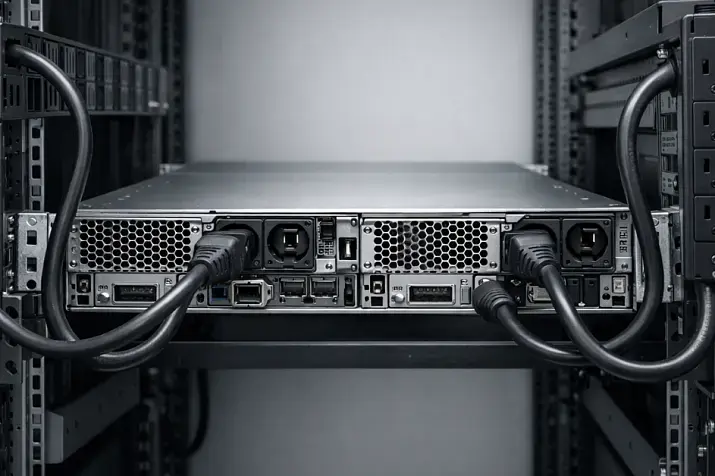
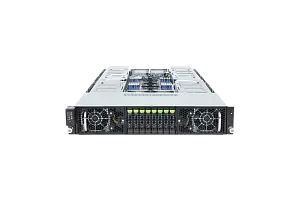
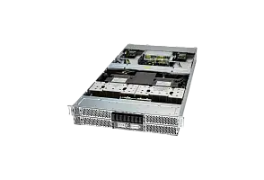
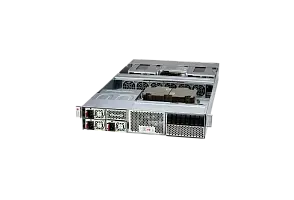
GPU servers
Common myths and mistakes
- “Gen always matters more than width” — no. It’s the combination: Gen × width × topology × uplink × NUMA.
- “If the slot is x16, it will be x16” — not necessarily: a slot can be physically x16 but electrically x8.
- “A PCIe switch solves everything” — it adds ports, but doesn’t remove uplink limits and adds latency.
- “Everything is the same in dual‑socket servers” — no: NUMA and inter‑socket traffic can turn “the same lanes” into very different latency and throughput.
Summary
- PCIe is generation + width + lane source (CPU/PCH) + topology.
- A physical “x16 slot” doesn’t guarantee an electrical “x16 link.”
- NVMe is almost always x4 — and many NVMe drives consume lane budget very fast.
- CPU lanes usually beat PCH lanes due to lower latency and fewer shared uplinks.
- In dual‑socket systems, locality (NUMA) can matter more than “formal bandwidth.”
- PCIe Gen5/Gen6 are demanding: risers/retimers/trace quality can make or break it.
- Switches help density, but require uplink/downlink math and an understanding of oversubscription.
- BIOS settings (bifurcation, Above 4G, IOMMU/ACS) can undermine the expected configuration.
- Modern platforms differ in lane budget: Xeon up to 80 PCIe 5.0 lanes, EPYC 9004 up to 128 Gen5 lanes.
- The best way not to miss — start not with “slots,” but with the block diagram and critical data paths.
How not to make a mistake when ordering/building
- Ask the vendor/integrator for the block diagram of the exact board/chassis/risers you’re buying (not a “similar model”).
- Explicitly define which devices must be on CPU lanes and where PCH/switch attachment is acceptable.
- Confirm which slots/backplanes belong to which socket (your NUMA plan).
- Verify BIOS supports the required modes (bifurcation, Above 4G, IOMMU/VT‑d/AMD‑Vi).
- For Gen5, pre‑approve risers/retimers and cooling (otherwise it’s “Gen5 on paper” but Gen4 in reality).